
A microwave oven is the key to 2-nanometer chip manufacturing
|
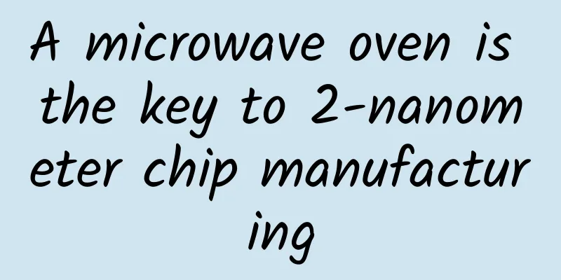
A home microwave oven modified by scientists is helping to create the next generation of cell phones, computers and other electronics, an invention that has proven to overcome a major challenge facing the semiconductor industry. The relevant research results were published in the scientific journal Applied Physics Letters under the title “Efficient and stable activation by microwave annealing of nanosheet silicon doped with phosphorus above its solubility limit”. James Hwang, professor of materials science and engineering at Cornell University, is one of the corresponding authors of the paper. (Source: Applied Physics Letters) As chips get smaller, silicon must be doped, or mixed, with higher concentrations of phosphorus to generate the required electrical current. Today, semiconductor manufacturers are reaching a limit where conventional methods of heating highly doped materials are no longer sufficient to produce stable semiconductors. Semiconductor maker TSMC thought microwaves could theoretically be used to activate excess dopants. But, just as a household microwave oven sometimes heats food unevenly, previous microwave annealing setups tended to create “standing waves” that prevented uniform activation of the dopants. Figure | Chip under an electron microscope (Source: Wikipedia) To this end, TSMC worked with Hwang to selectively control where the standing waves occur through a modified microwave oven, thereby activating the dopants just right without overheating or damaging the silicon crystal. "This discovery could be used to manufacture semiconductor materials and electronic products that will be produced around 2025," Hwang said. Even more, Hwang said: "Currently, only a few companies are producing 3-nanometer semiconductor materials. This new microwave method has the potential to enable chipmakers such as TSMC and Samsung to shrink the size to 2 nanometers." Photo: James Hwang (right) next to the modified microwave oven. It is reported that this breakthrough may change the geometry of transistors used in chips. For more than 20 years, in order to fit more transistors on each chip, transistors have been made to stand upright like dorsal fins. In recent years, chipmakers have begun experimenting with a new structure in which transistors can be stacked horizontally. Microwave annealing, which makes more doped materials possible, is key to making the new structure possible. References: https://aip.scitation.org/doi/10.1063/5.0099083 |
>>: It’s true that your brain stops working! Thinking can also make you tired!


Recommend
Bantang Mengyi Advanced Writing Camp, build a writing money printing machine from 0 to 1, worth 5999 yuan
Bantang Mengyi Advanced Writing Camp, build a wri...
Tesla: Tesla's car production in Q1 2022 was 305,400 and 310,000 were delivered
Tesla has just announced its car production and d...
Nokia is making a comeback, are European mobile phone brands looking to make a comeback?
Recently, a video about European mobile phone bra...
Product dilemma in brand marketing!
The acceleration of information exchange on the I...
How much does it cost to attract investment for Zhengzhou’s annual vehicle inspection mini program?
The advantages of WeChat mini program investment ...
Solid info! 6 customer acquisition models for APP promotion!
This time, I spent 2 days researching various pop...
How to operate Kuaishou short video on behalf of others?
Kuaishou is a short video platform that has enter...
As a newcomer to the industry, this is the most comprehensive industry learning strategy!
In the field of operations , a major difference b...
New efficacy of artemisinin, promising for treating this common disease
In 2015, Tu Youyou's team won the Nobel Prize...
Singapore autopsy found that the new coronavirus infection was not caused by the virus? This is a joke...
Recently, a rumor about the new coronavirus has s...
To achieve the goal of benefiting nature, these three conditions are needed to expand the scale of hybrid financing
Only by protecting nature can the world’s ambitio...
Five major mobile application development trends, is your app going astray?
Developers cannot ignore mobile app development i...
One bite of "overnight watermelon" contains 8,400 bacteria? Can you still eat it? The key is to look at these points
Experts of this article: Ruan Guangfeng, Director...
Teach you how to quickly get 99 points in event planning
Writing event strategy plans is the basic skill o...
Stay! New species are lurking around us
Seaside Lycoris Picture Bai Yu Baohua Old Crow Pe...